
In this article, I will talk about access to registers.
The following is the development environment at the time of posting.
PC: Windows 10 OS
IDE: STM32CubeIDE Version1.3.0
Configurator: STM32CubeMX Version5.6.0
Board: STM32Nucleo-F401RE
Accessing the registers
So far, I have only used HAL and Mbed and not code that directly touches the registers.
In my own opinion, HAL is very useful, so I will basically use it.
However, there are times when you want to touch the registers directly.
How should I write the code for such cases? I would like to take a look at this.
Please see RM0368 for the documentation for the microcontroller of the board I introduced.
Let’s look at the CR2 and CNT registers of the TIM2 general-purpose timer as an example.
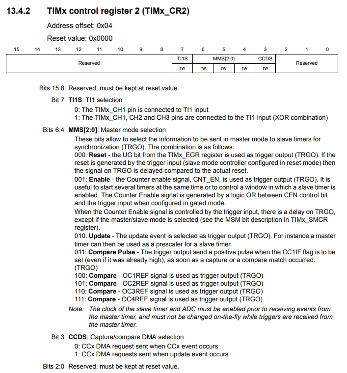
Section 13 describes the general-purpose timers TIM2-5, and Section 13.4.2 describes the TIM2-5 CR2 registers.
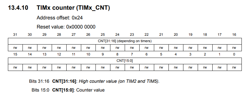
Section 13.4.2 describes the TIM2-5 CR2 registers, and Section 13.4.10 describes the TIM2-5 CNT registers.
The “rw” indicates that it is readable and writable.
The first way to specify a register is to go to Peripheral Functions->Registers.
Since we are discussing TIM2, for example, to specify the CR2 register in section 13.4.2 of the manual, use TIM2->CR2.
Similarly, to specify the CNT register in Section 13.4.10, use TIM2->CNT.
When there are multiple peripherals with the same function, such as timers and GPIOs, the peripherals will have a number on the end of the function or an alpha-byte (ABC…). for example.
Example.
Assume xxx is a register.
RTC->xxx
TIM2->xxx
GPIOA->xxx
Accessing with 32 bits
In the case of TIM2, this register is 32 bits, so to read the value, for example
To read the value, for example, uint32_t value = TIM2->CNT;
To read the value, for example, uint32_t value = TIM2->CNT;. To write the value, for example
TIM2->CNT = 0x00123456;
for example. The value to be written is written in hexadecimal notation, but it can be written in decimal or binary notation.
The value to be written is written in hexadecimal notation, but it can be written in decimal or binary notation. The arrow operator (->) indicates that the TIM2 part is a pointer.
If you look at stm32f401xe.h, you will see that TIM2 is defined as follows
#define TIM2 ((TIM_TypeDef *) TIM2_BASE)
It turns out that TIM2 is a pointer to a structure of type TIM_TypeDef.
The specific address can be found by following it from TIM2_BASE, but I’ll skip it here.
Looking at TIM_TypeDef, you can see that each register is a member of the structure.
typedef struct
{
  __IO uint32_t CR1;
  __IO uint32_t CR2;
  __IO uint32_t SMCR;
  __IO uint32_t DIER;
  __IO uint32_t SR;
  __IO uint32_t EGR;
  __IO uint32_t CCMR1;
  __IO uint32_t CCMR2;
  __IO uint32_t CCER;
  __IO uint32_t CNT;
  __IO uint32_t PSC;
  __IO uint32_t ARR;
  __IO uint32_t RCR;
  __IO uint32_t CCR1;
  __IO uint32_t CCR2;
  __IO uint32_t CCR3;
  __IO uint32_t CCR4;
  __IO uint32_t BDTR;
  __IO uint32_t DCR;
  __IO uint32_t DMAR;
  __IO uint32_t OR;
} TIM_TypeDef;
The other peripherals are defined in the same way, so you can see that they can be accessed by pointers in the structure as well.
It turns out that we can use the expression peripheral->register to access them.
Accessing bit by bit
In registers, bits are often separated by function.
In this section, we will look at control register 2 CR2 of TIM2.
Let’s start with a single bit setting.
Bit 7 of this register has a function called TI1S (probably short for TI1Select).
The purpose is to understand how to access it, so there is no need to understand its function.
Looking at stm32f401xe.h, TI1S of TIM2 is defined as follows.
#define TIM_CR2_TI1S_Pos (7U)
#define TIM_CR2_TI1S_Msk (0x1UL << TIM_CR2_TI1S_Pos)
#define TIM_CR2_TI1S IM_CR2_TI1S_Msk
Pos represents the position, which is at bit 7, hence 7U.
Msk means mask, which is the value 1 shifted 7 times to the left.
And TIM2_CR2_TI1S is the value of the mask itself, so to set TI1S to 1
TIM2->CR2 |= TIM_CR2_TI1S;
To set (clear) TI1S to 0, use a tilde to write TIM2->CR2 &= ~TIM2_CR2_TI1S_Msk;
In the above example, we used a single bit to determine whether to set 0 or 1. Next, let’s look at setting multiple bits.
Bits 6-4 of the register introduced above can be used to set the MMS (Master Mode Selection).
Since our goal is to understand how to access them, we do not need to understand their functions.
The macro for this part is defined as follows.
#define TIM_CR2_MMS_Pos (4U)
#define TIM_CR2_MMS_Msk (0x7UL << TIM_CR2_MMS_Pos)
#define TIM_CR2_MMS TIM_CR2_MMS_Msk
#define TIM_CR2_MMS_0 (0x1UL << TIM_CR2_MMS_Pos)
#define TIM_CR2_MMS_1 (0x2UL << TIM_CR2_MMS_Pos)
#define TIM_CR2_MMS_2 (0x4UL << TIM_CR2_MMS_Pos)
MMS has 3 bits, and there is no value to prohibit setting, so it can be set to a value from 0 to 7.
For example, to set 3, use
TIM2->CR2 &= ~TIM_CR2_TI1S_Msk;
TIM2->CR2 |= 3 << TIM_CR2_MMS_Pos;
To write 5, just change the 3 part to 5.
If you want to set multiple bits, you need to clear them first, unlike the case of 1-bit bits.
To set (clear) 0 in MMS, use a tilde
TIM2->CR2 &= ~TIM_CR2_MMS_Msk;
Creating a project
Start the IDE, select File- New – STM32 Project, when the Target Selection window comes up, select the Board Selector tab, select NUCLEO-F401RE from the Boards List and press the Next button.
Enter F401TIM2 as the Project name and press the Finish button.
It will ask “Initialize all peripherals with their default Mode ? Press Yes.
This kind of project is associated with the STM32CubeMx perspective. Do you want to open this perspective now ? Press Yes.
Enabling TIM2 in the code generator
In order to configure the register settings, you need to enable TIM2.
Click on Pinout & Configuration – Categories – Timers – TIM2.
In TIM2 Mode and Configuration – Mode, set Closk Source to Internal Clock and build to make sure there are no errors.
Coding
Write the following code after MX_TIM2_Init() in main().
MX_TIM2_Init();
  /* USER CODE BEGIN 2 */ TIM2
  TIM2->CNT = 0x12345678;
  TIM2->CR2 |= TIM_CR2_TI1S; // Set TI1S of CR2 to 1
  TIM2->CR2 &= ~TIM_CR2_TI1S_Msk; // set to 0

  TIM2->CR2 &= ~TIM_CR2_MMS_Msk;
  TIM2->CR2 |= 3 << TIM_CR2_MMS_Pos; // Set MMS of CR2 to 3
  TIM2->CR2 &= ~TIM_CR2_MMS_Msk; // set 0
Build and run
Make sure there are no errors after the build, then Run – Resume (F8 key).
With the program stopped, put a breakpoint on the line TIM2->CNT = 0x12345678;.
Run – Resume and the program will stop at the breakpoint.
Select SFRs on the right side of View, and select TIM2 in the register.
In addition, click on > in CR2 to expand CR2.
SFR stands for Special Function Register, which is a register for peripherals.
SFR stands for Special Function Register, which is a register for peripherals, while general-purpose registers can be checked by selecting Resigers.
I have drawn a red line through the part that I will focus on this time.
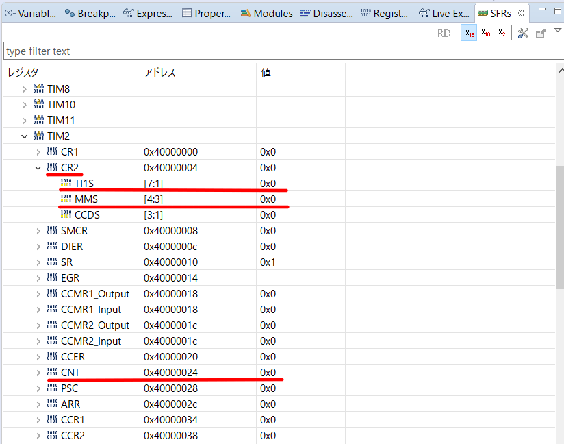
You can now check the value of the register.
Step Over (F6 key) and execute one line at a time to make sure that the value of each register is as you expect.
How did you like it?
Were you able to change the values of the registers as you expected?


